Low Noise Readout using Active Reset for CMOS APS
Boyd Fowler, Michael D. Godfrey, Janusz Balicki, and John Canfield
Affiliation: Pixel Devices International Inc.
Contact information:{fowler,godfrey,balicki,canfield}@pixeldevices.com;
Telephone: 408-616-8852; Fax: 408-616-8852
Abstract:
The fundamental detection limit on photodiode based CMOS image sensors is due to pixel reset noise. Reset noise in standard active pixel sensor (APS) is well understood and is of order kT/C. In this paper we present a new technique for resetting photodiodes, called active reset, which reduces reset noise without adding lag. Active reset can be applied to standard APS, uses bandlimiting and capacitive feedback to reduce reset noise. This paper discusses the operation of an active reset pixel. Measured results from a 6 transistor per pixel 0.35um CMOS implementation are presented. Measured results show that reset noise can be reduced to less than kT/18C using active reset.
Introduction:
Noise in CMOS image sensors is typically much larger than in CCDs. CMOS image sensors will not displace CCDs in the market until this fundamental problem is overcome. Image sensor noise can be categorized as either fixed pattern (FPN) [1] or temporal. FPN can be eliminated by using pixel to pixel offset and gain correction. On the other hand, temporal noise, after it is added to the image data, cannot be removed. Therefore techniques for reducing temporal noise in CMOS image sensors must be developed. Temporal noise in standard photodiode APS is well understood [2]. The largest temporal noise component is contributed by resetting the pixel, and is of order kT/C. In CCDs temporal reset noise is eliminated by using correlated double sampling (CDS) [6]. Due to space limitations, pixel level CDS cannot be used in APS. Pain et al. [4] present a photodiode reset technique called HTS that reduces reset noise to kT/2C without the addition of lag. Although this is a significant reduction in reset noise more is still required for CMOS sensors to compete with CCDs. In this paper we introduce a new technique for resetting the pixel, called active reset, that reduces reset noise without adding lag. Active reset can be directly applied to standard APS, uses bandlimiting and capacitive feedback to reduce reset noise. This paper discusses the operation of an active reset pixel; in addition, test results from a 6 transistor per pixel 0.35um CMOS implementation are presented. The remainder of this paper is organized as follows. The Operation section describes the basic operation of an active reset pixel. The Measured Results section presents measured data from a 6 transistor active reset pixel fabricated in a 0.35um CMOS process. Finally, in the Conclusion section we discuss the results and future directions for active reset.
Operation:
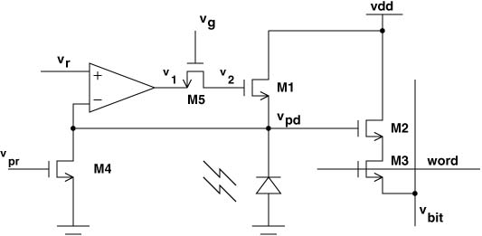
The general form of an active reset APS pixel is shown in Figure 1. It consists of two independent circuits, a readout circuit and a reset circuit. The readout circuit consists of two NMOS transistors M2 and M3, and the reset circuit consists of three NMOS transistors, M1, M5 and M4, and an amplifier.
 |
| Figure 1 |
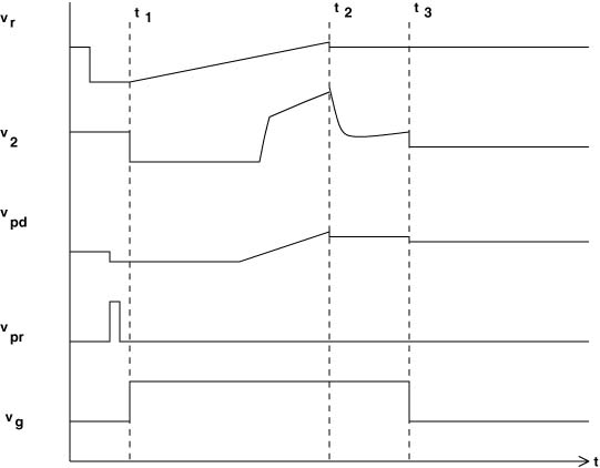
The operation and noise characteristics of the readout circuit have been thoroughly discussed in the literature [2,3]. Our focus in this paper is the reset circuit. Operation of the reset circuitry is as follows. Just before t_1, v_pr pulses for approximately 100ns and pulls v_pd to ground. Starting at t_1, v_g rises to v_dd and turns on M5, and v_r rises slowly, at about 0.1V/us, from ground to the maximum value of v_r at t_2. When v_r exceeds v_pd, the amplifier output rises and turns on M1. Then v_pd follows v_r until v_r stops rising and undershoots by a few tens of millivolts, at t_2, and v_pd overshoots v_r. v_pd overshoots v_r because M1 can only pull up and v_r has undershot its maximum value. After v_pd overshoots v_r, the output of the amplifier v_1 drops and turns M1 off. Now only the overlap capacitance of M1 is used to control v_pd. Finally, at t_3, v_g falls and turns off M5. This completes reset of the pixel. Reset waveforms are shown in Figure 2. Theoretical analysis presented by Fowler et al. [7] shows that the lag caused by active reset will be less than 0.1% of the maximum output swing (full scale). In addition by appropriately selecting the gain of the reset amplifier, the overlap capacitance of M1, and the bandlimiting capacitance of the amplifier, pixel reset noise will be much lower than kT/C. This reduction in reset noise is achieved by turning off M1, bandlimiting the reset amplifier, and by controlling the reset loop via a capacitive voltage divider.
 |
| Figure 2 |
Measured Results:
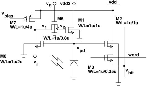
In this section, we present lag and noise measurements from a test sensor fabricated in a 0.35um standard digital CMOS process. Figure 3 shows a schematic of the active reset pixel. The measured capacitance of the photodiode is about 25.3fF. Lag measurements were performed using a 565nm green LED and an integrating sphere. The LED was placed at the input port of the integrating sphere and the sensor was placed at the output port.
 |
| Figure 3 |
The LED was pulsed with a 12.5Hz 50% duty cycle square wave. The pulse amplitude was adjusted to achieve a 1V pixel input-referred signal during a 10ms integration period. Five thousand measurements were used to estimate lag. Using this setup, we measured a lag of 0.02% of full scale. The optical and electrical setups used to measure noise are described by Fowler et al. [8]. The analog output of the sensor is amplified using a low noise amplifier (LNA) and digitized using a 16-bit ADC. All noise measurements were taken without illumination. When taking the noise measurements, we first determine the board-level noise, including the LNA noise and the ADC quantization noise. The measured output referred RMS board-level noise voltage was found to be 28.5uV RMS. Using the estimated gain of the follower, M2, and subtracting board-level noise, the input-referred RMS reset noise voltage was 96uV RMS. kT/C reset noise of a 25.3fF pixel is 406uV RMS, and therefore active reset reduces the RMS reset noise by 406/96 = 4.23, i.e. the reset noise power has been reduced to about kT/18C.
Conclusion:
We have shown that active reset can be used to lower reset noise to less than kT/18C without adding lag. This is nine times less noise power than reported in previous work [4]. Theoretical calculations show than reset can be reduced to less than kT/200C [7]. We plan to reduce the pixel level transistor count of active reset in the future and implement it in various sized 2D image sensors. We believe this will allow CMOS image sensors to achieve much lower read noise than even scientific grade CCDs at comparable pixel output data rates.
References:
[1] A. El Gamal et al., "Modeling and Estimation of FPN Components in CMOS Image Sensors", In Proceeding of SPIE, vol. 3301, San Jose CA, 1998.
[2] H. Tian et al., "Analysis of Temporal Noise in CMOS APS", In Proceeding of SPIE, vol. 3649, San Jose CA, 1999.
[3] O. Yadid-Pecht et al., "Optimization of Noise and Responsivity in CMOS Active Pixel Sensors for Detection of Ultra Low Light Levels", In Proceeding of SPIE, vol. 3019, San Jose CA, 1997.
[4] B. Pain et al., "Analysis and enhancement of low-light performance of photodiode-type CMOS active pixel imagers operated with sub-threshold reset", In Proceeding of 1999 IEEE Workshop on CCDs and AIS, Nagano Japan, 1999.
[5] S. Mendis et al., "Progress in CMOS Active Pixel Image Sensors", In Proceeding of SPIE, vol. 1994, San Jose CA, 1994.
[6] T. Nobusada et al., "Frame Interline CCD Sensor for HDTV Camera", ISSCC Digest of Technical Papers, San Francisco CA, 1989.
[7] B. Fowler et al., "Low Noise Readout using Active Reset for CMOS APS", In Proceeding of SPIE, vol. 3965, San Jose CA, 2000.
[8] B. Fowler et al., "Method for estimating quantum efficiency for CMOS image sensors", In Proceeding of SPIE, vol. 3301, San Jose CA, 1998.