OPTICAL/UV SINGLE PHOTON IMAGING SPECTROMETERS
USING SUPERCONDUCTING TUNNEL JUNCTIONS
C.M. Wilson, K. Segall, L. Frunzio, L. Li, D.E. Prober a
D. Schiminovich, B. Mazin, C. Martinb
R. Vasquezc
a Yale University, New Haven, Connecticut, USA
bCalifornia Institute of Technology, Pasadena, California USA
cNASA Jet Propulsion Laboratory, Pasadena, California USA
ABSTRACT
We report on the development of an "all-in-one" detector that provide spectroscopy, imaging, photon timing, and high quantum efficiency with single photon sensitivity: the optical/UV single-photon imaging spectrometer using superconducting tunnel junctions. Our devices utilize a lateral trapping geometry. Photons are absorbed in a Ta thin film, creating excess quasiparticles. Quasiparticles diffuse and are trapped by Al/AlOx/Al tunnel junctions located on the sides of the absorber. The Ta/Al interface does not overlap the junction area. Imaging devices have tunnel junctions on two opposite sides of the absorber. Position information is obtained from the fraction of the total charge collected by each junction. We have fabricated high quality junctions with a ratio of sub-gap resistance to normal state resistance greater than 100,000 at 0.22 K. We have measured the single photon response of our devices. For photon energies between 2 eV and 5 eV we measure an energy resolution between 0.47 eV and 0.40 eV respectively on a selected region of the absorber. We can estimate the number of pixels the device can resolve from the energy resolution. We find that these early devices have as many as 5 pixels per strip.
1 INTRODUCTION
There has been great interest in the concept of single photon spectroscopy in recent years. Two competing technologies are superconducting tunnel junctions (STJ) and transition edge sensors (TES) [1, 2]. These technologies may offer "all-in-one" detectors that provide spectroscopy, imaging, photon timing, and high quantum efficiency with single photon sensitivity at energies ranging from the infrared to the gamma ray. In the optical/UV region, much attention has been focused on imaging spectrometers. The general approach pursued to date is large format arrays of single-pixel detectors [3].
We propose to develop STJ detectors with intrinsic imaging, meaning that the detectors have many more pixels than read out channels [4, 5]. We do this using STJ detectors with lateral trapping. This work is an extension of successful x-ray work, where we have made detectors with a resolution of 15 eV referred to a 6 keV x-ray [6, 7, 8].
2 OPERATING PRINCIPLE
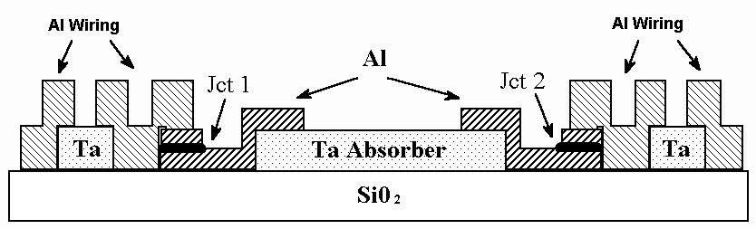
Fig. 1 shows a schematic drawing of an imaging STJ detector. Many physical processes are involved in the operation of these detectors [9]. First, an incident photon is absorbed in the central Ta film breaking Cooper pairs and creating quasiparticles. The quasiparticles diffuse until they reach the Al. In the Al, they can scatter inelastically, losing energy until they reach the Al gap. Once the quasiparticles scatter below the gap of Ta, they are "trapped" in the Al electrode. The quasiparticles then tunnel and are read out as an excess sub-gap current. The current pulses are then integrated to obtain a charge from each junction, Q1 and Q2. We have the relation
where Ephoton is the photon energy and D Ta is the energy gap of Ta.
 |
| Figure 1. |
The fraction of charge collected in each junction tells us the location of the absorption event. If the photon is absorbed in the center, then the charge divides equally. If the photon is absorbed at one edge of the absorber, then the closest junction collects most of the charge. In the limit of no absorber loss and perfect trapping
where L is the length of the absorber, DL is the uncertainty in the position and DE is the uncertainty in energy [10].D L can be considered the effective size of a pixel.
Another important process in our detectors is backtunneling. Considering one half of Fig. 1, we have a lateral Ta/Al/AlOx/Al/Ta tunnel junction. We inject excited quasiparticles into the Al trap from the Ta absorber. At high bias voltages, quasiparticles in the Al trap can only tunnel directly to the counter electrode. The high Ta gap then confines excited quasiparticles near the tunnel barrier. The confined quasiparticles in the counter electrode can then undergo a pair-mediated tunneling process called backtunneling. When a quasiparticle backtunnels, a pair in the trap is broken. One electron from the pair tunnels to the counter electrode and recombines with the (backtunneling) quasiparticle in the counter electrode. The remaining electron in the trap is promoted to be a quasiparticle in the trap. So, the net result is that a quasiparticle is transferred from the counter electrode to the trap against the bias. However, a charge is simultaneously transferred in the forward direction with the bias. Although backtunneling seems like a complicated process, it has the same probability as direct tunneling.
Keeping both processes in mind, we see that a confined quasiparticle can circulate, tunneling and backtunneling. Because both tunneling and backtunneling transfer a charge in the forward direction, this effect gives the junctions charge gain. Thus, we measure an integrated charge many times greater then the number of quasiparticles initially created.
We have designed our present devices to maximize backtunneling by interrupting the Al wiring with Ta plugs. The absorber and the plugs confine the quasiparticles near the junction.
3 EXPERIMENTAL CONDITIONS
All devices have been fabricated at Yale in a high vacuum deposition system with in-situ ion beam cleaning. We start with an oxidized Si substrate. The Ta absorber and plugs are then sputtered at 750 ˚C. Next a Nb ground contact is sputtered. The Al trilayer is then evaporated in one vacuum cycle. A SiO insulating layer is evaporated and finally Al wiring is evaporated. An in-situ ion beam cleaning is performed before each metal deposition to ensure good metallic contact. All layers are patterned photolithographically using either wet etching or lift-off.
Measurements are made in a two stage 3He dewar. The base temperature is 220 mK.
To measure the photo-response of our junctions, we use a room temperature JFET current amplifier. We use an Amptek A250 amplifier with a 2SK146 input transistor. Extra circuitry is added that allows the A250/2SK146 to be dc coupled to the junction [11]. The amplifier thus provides an active voltage bias for the junction.
We illuminate the detectors using a small Hg lamp calibration source. A bandpass filter selects one photon energy at a time. We bring light into the dewar using an optical fiber. The fiber is UV grade fused silica. The fiber is Al coated to enhance UV transmission up to energies of 6 eV. The filtered light passes through a fiber splitter that divides the light equally between two fibers. One of these fibers is fed into the dewar. The other fiber is fed into a photomultiplier tube that simultaneously measures the intensity.
4 RESULTS
We have had success fabricating high quality thin films. We have made Ta films with a residual resistance ratio of 17. We have also measured a quasiparticle loss time of 450 ms at 220 mK. This loss time can be compared to a time of ~10 ms needed for a quasiparticle to diffuse across the absorber and be trapped in the Al junctions. We have made Al films with a residual resistance ratio of 12. We have measured a quasiparticle loss time of 160 ms at 220 mK in these Al films. This loss time can be compared to the ~ 2 ms tunnel time in a typical junction.
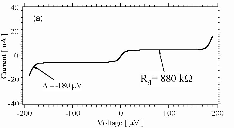
We have also made outstanding junctions. Two characteristics are important for low noise. First, junctions should have a low sub-gap current to minimize shot noise. They should also have a large sub-gap resistance to minimize the contribution of amplifier voltage noise. Figure (2a) shows the sub-gap I-V curve of a 400 mm2 junction with a normal state resistance of R NN = 2.3 W. At 220 mK we measure a sub-gap current of ~5nA and a sub-gap resistance of 880 k
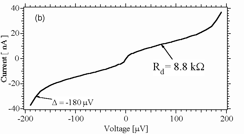
W. The sub-gap resistance exceeds our expectations by an order of magnitude.Unfortunately, we have had difficulty reproducing these high quality junctions when they are integrated into a complete detector with backtunneling. Figure (2b) shows the sub-gap curve of a 100 m m2 junction from a different fabrication run, which is integrated into a working detector. This junction has a normal state resistance of RNN = 13.8 W. In this figure, the sub-gap resistance is only 8 kW. We believe that the excess current may be caused by stray photons coupled down the leads. In fact, we were able to reduce the excess current by as much as a factor of 3 by placing the dewar in an electromagnetically-shielded enclosure.
 |
 |
| Figure 2. | |
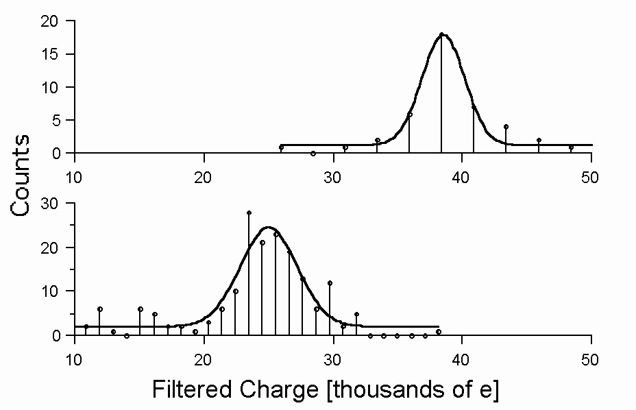
We have detected optical and ultraviolet photons using a detector with junctions as in figure (2b). This device has a Ta absorber 10 mm wide by 100 mm long by 0.6 microns thick. Each Al trap overlaps the absorber by 5 mm. In figure (3), we show two histograms of events recorded with this detector Figure (3a) and (3b) are the response to illumination with 4.89 eV ultraviolet photons and 2.27 eV green photons, respectively. We have plotted the number of events versus the collected charge. The raw current pulses were digitally filtered before being integrated to obtain the charge measurements.
The full width at half maximum (FWHM) of the UV histogram is 0.4 eV. The full width at half maximum (FWHM) of the green histogram is 0.47 eV. The histograms in figure (3) contain events from a limited range of the absorber. This gives us a resolving power of R = 12 at 4.89 eV and of R = 4.8 at 2.27 eV. These resolving powers can be compared to the theoretical limit for devices with backtunneling: R = 25 and R = 17 at 4.89 eV and 2.27 eV respectively.
 |
| Figure 3 |
The resolution over the whole absorber, under UV illumination, is 1.5 eV, for a resolving power of R = 3.5. An energy resolving power of R=3.5 in the UV implies that the detector can resolve 5 spatial pixels. This particular detector has an active absorber area 70 mm long by 10 mm wide. So, the detector has 5 pixels with dimension 14 mm by 10 mm. This is achieved with only two readout channels.
We have measured the noise spectra of both junctions with no illumination and they are consistent with the measured resolution. However, the noise spectra contain excess noise that we do not fully understand at present. The noise is clearly associated with the excess current that we see in the junctions; the excess noise changes as the excess current changes. However, the spectral density of the noise (Amps2/Hz) exceeds the expected shot noise density of the excess current by more than an order of magnitude. In addition the noise is not white, but instead rolls off above a few kilohertz. This roll-off frequency varies with the bias condition. Both the excess noise and the low frequency roll-off are consistent with the current and noise being caused by stray photons absorbed in the device. Because the photons would produce charge in large bunches, the effective charge in the standard shot noise formula would be larger [12]. In addition, the noise should have the spectral shape of a photon induced pulse, and the noise spectrum is consistent with this. We thus plan to further improve the shielding and filtering of the measurement setup to eliminate this excess noise.
The fall time of the photon pulses contains important physical information. We have measured the fall time by averaging 2000 single UV photon pulses and fitting an exponential to the waveform. A simple physical model tells us that the fall time of the pulse should be the quasiparticle loss time in the Al junctions. Basically, since the quasiparticles are confined near the junctions by the Ta plugs, they continue to tunnel and backtunnel until they are lost. We measure a quasiparticle loss time of tloss = 159 ms.
The average number of times that a quasiparticle tunnels is
where ttunis the tunnel time. We can extract the tunnel time from measurements of R NN. We measure ttun = 2.46 ms. With this we find that n = 65. We estimate that the initial charge created by a 4.89 eV photon is about Qo = 4000 e- [13]. The total charge we collect is about Qtotal = 240,000 e- . So, the addition of the Ta plugs in the wiring does produce a large charge gain.
5. CONLUSIONS
We have begun the development and testing of imaging, single photon spectrometers. Our devices use superconducting tunnel junctions with lateral trapping. Our preliminary fabrication results are very promising. We have detected single optical and UV photons with these first detectors.
6 REFERENCES
1. "Superconducting Particle Detectors" N.E. Booth and D.J. Goldie, Supercond. Science and Technology 9, 493 (1996).
2. "Detection of Single IR, Optical and UV Photons Using Superconducting Transition Edge Sensors" B. Cabrera et al., Applied Physics Letters 73, 735 (1998).
3. "On the Development of a STJ Camera for Ground-Based Optical Astronomy" N. Rando et al., Proc. SPIE 3435 (1998). N. Rando et al., Proc. SPIE 4008, to be published
4. "Optical/UV single-photon imaging spectrometers using superconducting tunnel junctions" C.M. Wilson, et al., Nucl. Inst. Meth. A 444, 449 (2000).
5. P. Verhoeve, et al., Proc. SPIE 4008, to be published.
6. "Single-photon imaging x-ray spectrometers" K. Segall et al., IEEE Trans. Appl. Supercond., 9, 3326 (1999).
7. "Experimental quasiparticle dynamics in a superconducting, imaging x-ray spectrometer" S. Friedrich et al., Appl. Phys. Lett. 71, 3901 (1997).
8. D.E. Prober, this conference
9. "Noise mechanisms in superconducting tunnel-junction detectors" K. Segall et al., Appl. Phys. Lett. 76, 3998 (2000).
10. H Kraus et al., Physics Letters B 231, 195 (1989).
11. S. Friedrich et al., IEEE Trans. Appl. Supercond. 7, 3383 (1997).
12. Le Grand et al., Proc. 7th Int. Workshop on Low Temp. Detectors, 106 (1997).
13. N. Rando et al., Nucl. Inst. Meth. A 313, 173 (1992).