256x256 GaN Ultraviolet Imaging Array
Ted Z.C. Huang, Shahid Aslam, Anh La, D. Brent Mott, Laddawan
Ruamsuwan
Detector Systems Branch, Goddard Space Flight Center
Charles Joseph / Department of Physics and Astronomy, Rutgers University
Dennis Wickenden, Applied Physics Laboratory
ABSTRACT
We have successfully developed a prototype 256x256 photoconductive GaN ultraviolet (UV) imaging array. The array, with its 30x30 m m2 pixels indium bump bonded to a Lockheed Martin Fairchild Systems LT9601 readout integrated circuit, is sensitive to ultraviolet light below 365 nm with a sharp reduction in response to visible light. The array was installed into a custom designed UV camera utilizing a Nikon UV lens with all the off-chip electronics interfaced to an automatic computer controlled system. To the best of our knowledge, this is the first reported UV array camera based on the nitride materials.
1. INTRODUCTION
Wide band gap materials, primarily SiC and III-V nitride materials, have attracted extensive interest during the past few years for their applications in making light emitting devices, high-power and high-temperature electronic devices, and ultraviolet detectors. There has been a strong demand for compact solar-blind, solid-state ultraviolet (UV) photodetectors for room temperature operation. The use of III-V nitrides for photodetector applications is expected to yield high responsivities with low dark currents over a wide range of temperatures. GaN and aluminum nitride (AlN) have direct bandgaps of 3.4 and 6.2 eV, respectively, with corresponding cutoff wavelengths of 365 and 200 nm. Since they are miscible with each other and form a complete series of aluminum gallium nitride (AlGaN) alloys, it should be possible to develop detectors with wavelength cutoffs anywhere in this range.
During the past few years, prototype nitride-based single element photodetectors and linear arrays have been fabricated and studied by several groups1-5. It was commonly reported that the detector performance varied from sample to sample depending on the material quality. Although these materials show great promise, more work is needed to develop their quality to their full potential. Despite the need for continued research, these materials have reached sufficient maturity to warrant a vigorous device development effort to create UV image sensors. In this work, we report our success in making a GaN array and UV camera using metal-semiconductor-metal (MSM) structures.
2.
DEVICE PROCESSING
The starting material was a 1.5 µm undoped layer of GaN grown on a sapphire substrate. The MSM photoconductive 256x256 array with a pixel size of 30x30 mm2 was patterned by conventional photolithographic lift-off techniques. Each pixel consists of two ohmic metal contacts made by evaporating 20 nm of titanium followed by 30 nm of aluminum and capping with 120 nm of gold, and annealed at 450oC for 10 min in a N2 environment. After the MSM structures were delineated, indium bumps were deposited on the contacts, the wafers diced into individual arrays, and the arrays mated to a Lockheed Martin Fairchild Systems LT9601 readout integrated circuit (ROIC). Voltage bias is applied by the ROIC to a bias grid common to all pixels, and the signal current is read by the ROIC from the center contact individual to each pixel.. Incident light illuminates the GaN array through the back side, i.e. sapphire substrate side, and the readout system was indium bump bonded to the front side. An array mated to its ROIC is shown in Figure 1.
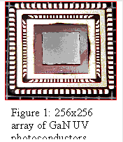 |
| Figure 1 |
The array with ROIC was then mounted in a specially designed camera, as shown in Figure 2. The camera utilizes a commercial Nikon UV lens and has the capability of operating at various temperatures ranging from 250K to room temperature. Photoconductors were chosen over photodiodes to take advantage of the photoconductive gain to produce a more sensitive array.
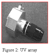 |
| Figure 2 |
Figure 3 shows the image taken by the GaN array camera. A commemorative pin was placed in front of the camera and was illuminated by broadband light from a Xenon lamp. The images are the reflection of UV light from the pin.
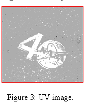 |
| Figure 3 |
3. DEVICE RESULTS
Figure 4 shows the mean spectral responsivity from a GaN ultraviolet array detector (wafer No. 706241) at room temperature and a flood illumination (no lens) from a monochrometer. The array is under a nominal bias of 3 V. The data shown were averaged from two 20x20 sub-arrays selected near the center area of the array. The responsivity of the GaN array is of the order of 2-3 A/W in the region between 300 nm and 360 nm, and the array shows a visible light rejection of almost three orders of magnitude. The magnitude of the spectral responsivity curve is much smaller than expected from the spectral responsivity measured on individual elements. By using a microprobe station to measure individual pixels from the same wafer, we have obtained a responsivity of 690 A/W at 365 nm under a bias of 5V. Because the current to voltage transfer function of this particular ROIC has not been measured, the actual responsivity of the GaN array is not a reliable number at this time. It should also be pointed out that the responsivity of detectors vary greatly from wafer to wafer and across a wafer. We have fabricated tens of wafers, and the responsivities ranges from 2.5 to 3200 A/W. The array detector reported in this paper was not chosen based on the best material quality, but on the yield of fabrication and the yield of indium bump bonding.
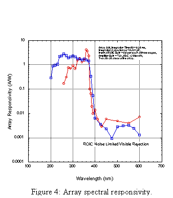 |
| Figure 4 |
ACKNOWLEDGMENTS
We thank Mr. Thomas Hartmann and Jay Cho for design and manufacture of the GaN UV camera.
REFERENCES
1. M.A. Khan, J.N. Kuznia, D.T. Olson, J.M. Van Hove, M. Blasingame, and L.F. Reitz, "High-responsivity photoconductive ultraviolet sensors based on insulating single-crystal GaN epilayers," Appl. Phys. Lett., 60, 2917, 1992.
2. D. Walker, X. Zhang, P. Kung, A. Saxler, J. Javadpour, J. Xu, and M. Razeghi, "Kinetics of photoconductivity in N-type GaN photodetector," Appl. Phys. Lett., 68, 2100, 1996.
3. Q. Chen, M.A. Khan, C.J. Sun and J.W. Yang, "Visible-blind ultraviolet photodetectors based on GaN p-n junctions," Electron. Lett., 31, 1781, 1995.
4. Z.C. Huang, J.C. Chen and D. B. Mott, "Improved performance of GaN ultraviolet detectors,” J. Electron. Mater., 26, 330, 1997.
5. Z.C. Huang, J.C. Chen, D.B. Mott and P.K. Shu, "High performance GaN linear array," Electron. Lett., 32, 1324, 1996.