A Wide Energy Band Compound Pixelated Photon Detector
Upendra Desai, Larry Orwig Code 682, NASA/GSFC
We present a new concept of a stacked detector that provides high spectral resolution over a wide energy band (keV-MeV). The concept is to use detectors of appropriate energy bandwidth to avoid saturation effects of single detectors normally used. It also provides identification whether the interaction is photoelectric or compton interaction. Multiple comptons can also be identified. It enables rejection of energetic particle tracks. For the energy range from sub keV to 20 keV we use silicon PIN detectors. To cover energies from 20 keV to 60 keV we use a 2-mm-thick CZT detector beneath the "Si" PIN detector. To extend the energy range above 60 keV we incorporated another 5-mm-thick CZT. To achieve the response to MeV photons we incorporate a 2-cm-thick scintillator viewed by a PIN photo diode as the last element of the stack. The significant advantages of this concept over a single detector would be (1) charged particle rejection capability, (2) low internal noise, and (3) identification of Compton interactions.
Over
the last couple of years, a significant improvement in energy resolution of
solid-state detectors for soft and hard x-rays has been achieved. Even at room
temperature, one can achieve less than one keV resolution in
commercially available silicon diodes for soft x-rays up to 15 - 20 keV. With
a thermoelectric cooling, one can achieve resolution of 150 eV for silicon
detectors for soft x-rays. High 'Z' solid state detectors like Cadmium Zinc
Teluride (CZT) are also available commercially, providing less than 2 keV
resolution at 122 keV. This is made possible primarily because of very low
leakage currents of the detectors with high resistivity improved materials,
and low capacitance because of their small sizes. These detectors are
presently available in sizes less than one cm2 area. The size and
the thickness of these detectors are major limitations for their use in wide
band energy measurements. We have evaluated silicon diode detectors with 1 cm2
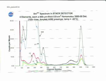
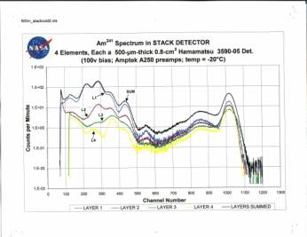
area and thickness from 300 μm to 2 mm. In 1996, we evaluated a stacked
configuration of silicon detectors to increase detector efficiency at higher
energies as well as to reduce the charged particle contribution. The stacked
configuration also provides the capability to reduce pile up problems
encountered in a single wide energy hand detector. When the spectrum to be
observed is steep (power law index of -3 to -5), saturation of the detector is
a very serious problem in the deconvolution of the data. Measurements made in
narrow energy bands by individual members of the stack avoid this problem. The
stacking enables one to identify whether there was a photoelectric
interaction, as revealed by a response in only one element of the stack or a
Compton scattering as recorded by signals in multiple elements of the stack.
We
propose now to use different detector elements in a stacked configuration to
enhance the total energy bandwidth. We propose to have silicon elements for
low energy photons - below which we propose to use CZT elements to cover
energies up to 100 keV. To achieve high detection efficiencies up to a few
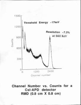
tens of MeV, we propose to have a CSI scintillator viewed by an avalanche
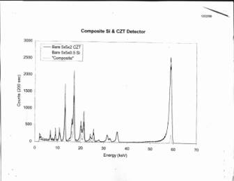
photo-diode (APD). We have evaluated all the individual elements - Silicon
PINs (thin & thick), CZT (2 mm -5mm thickness), and CSI (4 cm x 1 cm x 1
cm). The single pixel area would then be 1 cm x 1 cm covering the energy range
from a keV to 10 MeV. The resolution in the 1 - 15 keV band will be sub keV in
the silicon detectors. CZT will offer high detection efficiencies up to 200 -
300 keV with an energy resolution of a few keV. The last element, a CSI
scintillator viewed by a avalanche photo-diode (APD) provides high detection
efficiency for photons with energy up to 10 MeV. The energy resolution at 660
keV is around 10%.
|
|
|
|