|
| NICMOS Instrument Handbook for Cycle 11 | |||
|
|
Detector Characteristics
Overview
Each NICMOS detector comprises 256 x 256 square pixels, divided into 4 quadrants of 128 x 128 pixels, each of which is read out independently. The basic performance of the nominal flight detectors is summarized in Table 7.1. Typically, the read-noise is ~30e-/pixel. Only a few tens of bad pixels (i.e., with very low response) were expected, but particulates-possibly paint flakes-have increased this number to >100 per detector. The gain, ~5-6 e-/ADU, has been set so as to map the full useful dynamic range of the detectors into the 16-bit precision used for the output science images.
Table 7.1: Flight Array Characteristics Dark Current (e- /second)1 0.4-2.0 0.4-2.0 0.4-2.0 Read Noise (e-)2 ~30-35 ~30-35 ~30-35 Bad Pixels (including particles) 213 (.33%) 160(0.24%) 139(0.21%) Conversion Gain (e- / ADU) 5.4 5.4 6.5 SATURATION (e-)3 (98% Linearity) 145,000 145,000 185,000 50% DQE Cutoff Wavelength (microns) 2.55 2.53 2.52
1 The dark current strongly depends on whether the "bump" anomaly will be observed or not (see next section) when NICMOS will be cooled down to operating temperatures with the NCS.
2 The quoted readout noise is the realized noise from a pair of readouts (i.e., the quadrative sum of a single initial and final readout). The following sections will give more information for each of the quantities of this table.
3 Saturation is defined as 2% deviation from quadratic non-linearity.
Dark current
A NICMOS exposure taken with the blank filter in place should give a measure of the detector dark current. However, the signal in such an exposure consists of three different components: amplifier glow, shading, and linear dark current. The linear dark current is the current produced by the minority carriers inside the detector material. It increases linearly with exposure time, hence the name. It can be measured after subtraction of amplifier glow and correction for shading, both of which we will describe in the next section. The linear dark current was carefully monitored throughout the NICMOS warm-up at the end of Cycle 7N in order to estimate its value for operation under the NCS. Special care was taken to minimize the impact of those measurements that were affected by cosmic ray persistence after passage through the South-Atlantic Anomaly (see Chapter 4). The mean dark current of all three NICMOS chips for the whole temperature range of the warm-up is plotted in Figure 7.4. The characteristic increase and subsequent decline of the dark current between 75 and 85 K is an unexpected feature which is commonly referred to as the "bump".
Figure 7.4: NICMOS linear dark current as function of detector temperature. Upper plot presents NICMOS end-of-life (EOL) data with bump, and lower plot shows the dark current with the bump interatively removed.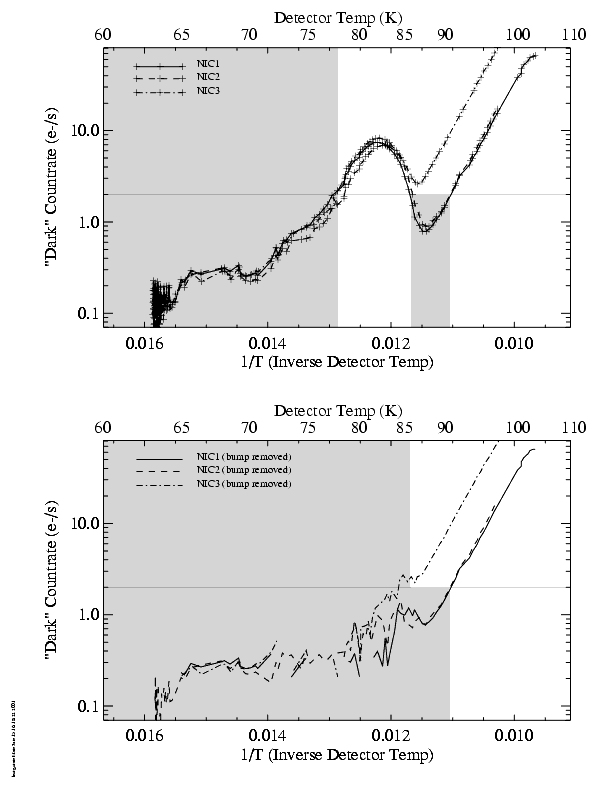
The theoretical expectation for the dark current at temperatures above ~ 140 K is to follow the charge carrier concentration, which rises with temperature according to the Boltzmann factor e-E/kT. At temperatures between 90 and 140 K, generation-recombination models provide the best agreement with laboratory measurements. The two regimes both produce a basically linear relation of log(dark current) vs. 1/T, but with different slopes. At temperatures below 90 K, poorly understood tunneling effects are known to cause a deviation from the generation-recombination model. These result in a flattening of the dark current decrease towards colder temperatures, until a basically constant dark current is reached. Except for the bump, the NICMOS dark current follows these general trends, as demonstrated in Figure 7.4.
The "bump"
The excess signal responsible for the bump shows the flatfield morphology (see NICMOS ISR 99-001 for more details). Moreover, the small specks of black paint known as "grot" are not visible in the bump images. Taken together, these observational facts suggest that some amount of excess charge was released inside the detector material, and subsequently picked up by the pn-junctions. The idea of an additional component to the normal "linear" dark current is also supported by the fact that subtracting a scaled flatfield exposure - constructed from the set of calibration flats and weighted by the DQE curve appropriate for the respective temperature - effectively flattens the dark current image, and smoothly interpolates the dark measurements before and after the bump (lowest line in Figure 7.4). A possible explanation for this additional signal component are low-energy electronic states ("traps") inside the detector material which can be produced, for example, either by the manufacturing process, or by cosmic ray bombardment. These traps were presumably filled during the ~ 4 year long "cold period" of the instrument during which the detectors were at temperatures around 60 K. The trapped charge was only released when the detectors warmed up through 75 K during the end-of-cryogen warmup. A laboratory test program designed to investigate the trapped charge theory and conducted at the University of Arizona, however, did not reproduce this signal (NICMOS ISR 00-002). Therefore, the exact dark current levels of the NICMOS detectors during Cycle 11 remain uncertain at this time.
The NICMOS Exposure Time Calculator (ETC) allows the user to choose between two dark current levels which reflect the best (0.5e- /s/pixel at 75 K) and worst (2e- /s/pixel at 78 K) case scenarios. Phase I proposers are recommended to use the worst case scenario (default ETC setting) for their exposure time calculations because of the current uncertainty for the NCS/NICMOS on-orbit performance. Orbit allocations derived from optimistic dark current estimates will NOT be adjusted if the dark current is indeed elevated above the assumed levels. We also point out that for most proposals, the difference between the two scenarios is negligible, as shown by the sensitivity curves in Appendix 1. This is because only the longest NICMOS exposures at wavelengths shorter than ~1.7 µm are in fact dark current limited.
Flat fields and the DQE
Uniformly illuminated frames taken with the NICMOS arrays show response variations on both large and small scales. These fluctuations are corrected in the normal way by flat fielding, which is an essential part of the calibration pipeline. In order to monitor the flat field structure of the NICMOS detectors, a large program of calibration lamp and earth flats was executed during Cycle 7 and throughout the warm-up. At the NICMOS temperatures achieved during Cycle 7, the flat field exposures showed considerable spatial structure, i.e. the relative responsivity of individual pixels varied by a large amount. Peak-to-peak variations between the highest and lowest sensitivity areas on the array were as much as a factor of 5 at 0.8 microns. The amplitude of the variations declines both with increasing wavelength and temperature. For the detector temperatures expected for Cycle 11, the flat field response will vary by a factor of ~2.5 (2) at the short (long) end of the NICMOS wavelength range.
The detective quantum efficiency (DQE) monitoring program during the warm-up of the instrument was designed to determine what exactly the response function of the NICMOS detectors at the NCS operating temperatures will be. Expectations were that low sensitivity pixels would experience a significant increase in DQE, especially at shorter wavelengths. Figure 7.5 shows the pixel response of all camera/filter combinations that were used during the monitoring (details of the data reduction are found in NICMOS ISR 99-001).
For all regions, the DQE increases roughly linearly between 63 K and 78 K, with a small curvature term. In all cameras, the linear slope is higher than average for low sensitivity regions, and lower than average for high sensitivity regions. This behavior effectively flattens out the DQE variations across the array, relative to Cycles 7 and 7N. The average responsivity at 75 K increased by about 45% at J, 33% at H, and 17% at K. The resulting wavelength dependence of the expected DQE for NICMOS operations at 78 K is shown in Figure 7.6. Here, we have scaled the pre-launch DQE curve, which was derived from ground testing of the detectors, to reflect the changes measured at the wavelengths used in the monitoring program.
Figure 7.5: DQE variations with temperature for all camera/filter combinations of the monitoring program. The coefficients of a second order polynomial fit are listed on the top left of each plot. For each dataset, the three curves depict a low sensitivity region on the chip (highest curve), the median DQE over the full chip (middle curve), and a high sensitivity region (bottom curve). Note also that the %DQE increase is larger for shorter wavelengths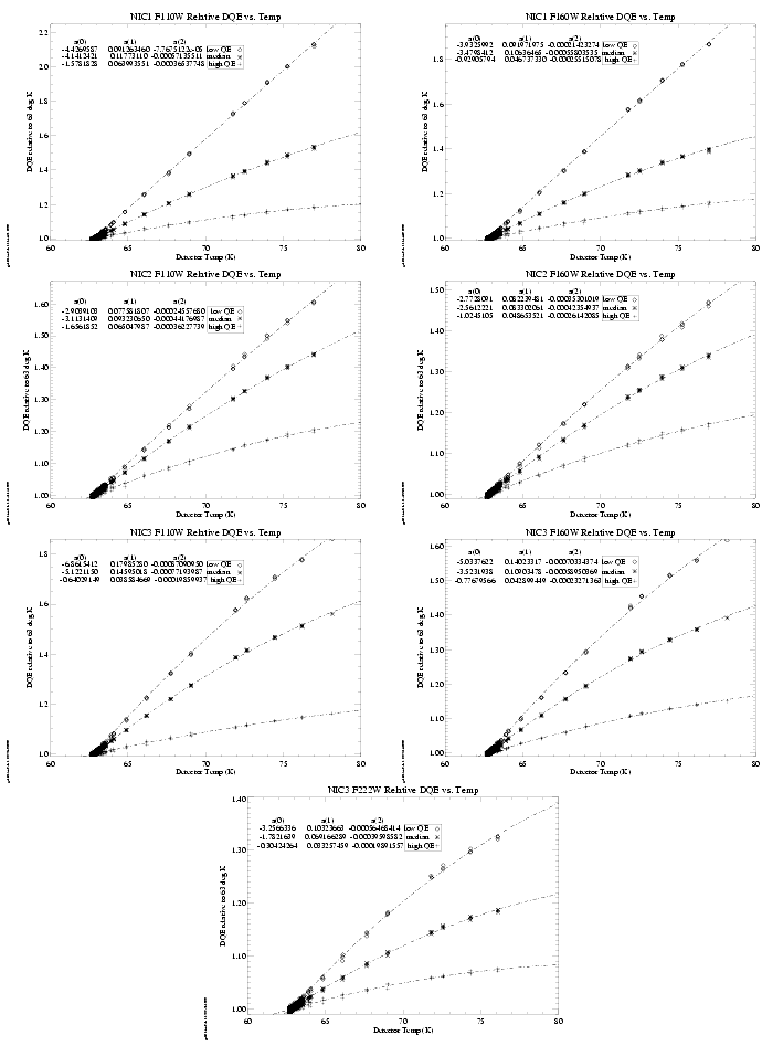
Figure 7.6: Expected NICMOS DQE as a function of wavelength for operations at 78 K (crosses), compared to pre-launch measurements.
The fine details in these DQE curves should not be interpreted as detector features, as they may be artifacts introduced by the test set-up. At the blue end, near 0.9 microns, the DQE at 78 K is ~20%; it rises quasi-linearly up to a peak DQE of ~90% at 2.4 microns. At longer wavelengths, it rapidly decreases to zero at 2.6 microns. The NICMOS arrays are blind to longer wavelength emission. Figure 7.7 shows the ratio of the DQE at 78 K to the DQE at 63 K, as a function of wavelength. The continuous line is extrapolated from the average measured in the three cameras during the warm-up monitoring for a subset of wavelengths (filters). When looking at these DQE curves, the reader should bear in mind that this is not the only criterion to be used in determining sensitivity in the near-IR. For example, thermal emission from the telescope starts to be an issue beyond ~1.7 µm. The shot-noise on this bright background may degrade the signal to noise obtained at long wavelengths, negating the advantage offered by the increased DQE.
Figure 7.7: The ratio of the expected DQE at 78 K to the DQE at 63 K for the three NICMOS cameras. The symbols are measurements. The continuous line is a linear extrapolation.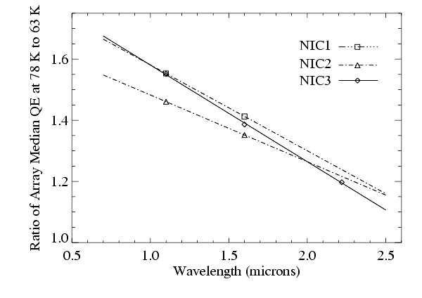
It is important, especially for observations of very faint targets for which the expected signal to noise is low, to note that the DQE presented here is only the average for the entire array. The flat field response is rather non-uniform, and thus the DQE curves for individual pixels may differ substantially. To demonstrate this, we plot the relative response of four selected detector areas in Figure 7.8. Each region consists of three adjacent pixels, either in a line or in an "L" shape. Two of them have relatively high sensitivity, and the other two show a lower than average sensitivity. The pixel sensitivity relative to the average over the entire array is plotted versus wavelength, using a number of 10% bandwidth measurements. For many pixels, the response variation is fairly slow between 1.0 and 2.2 microns. However, at about 2.25 microns, there is a pronounced turnover, beyond which the change with wavelength is significantly larger. Note, however, that these data were taken at temperatures around 60 K.
Figure 7.8: Relative Response as a function of wavelength of three-pixel groups. The curves show the DQE of individual pixels relative to the mean DQE for the entire array, for low- (top panel) and high sensitivity pixels (bottom panel).
The steeper gradient in the flat field response longward of 2.25 microns is likely to somewhat degrade the photometric accuracy of observations in the longest wavelength NICMOS filters. However, In Cycle 11, the NICMOS detector arrays are expected to be much flatter compared to Cycle 7 because of the stronger DQE increase with temperature of the low-sensitivity pixels described above. Figure 7.9 demonstrates this effect. As can be seen from the histograms on the right, the overall spread in pixel response values is much smaller at the temperatures expected for Cycle 11. Therefore, the photometric accuracy at the long wavelength end should be improved. Nevertheless, special care should be taken when observing sources with extreme colors (see Chapter 4).
Figure 7.9: Normalized flat field exposures of all NICMOS detectors, taken through the F110W filter at temperatures of 62 K (left) and 78 K (right). The grayscale stretch is the same for both temperatures in each camera. The histograms on the right show the "flattening" of the arrays at the higher temperature which can also be seen by comparing the images.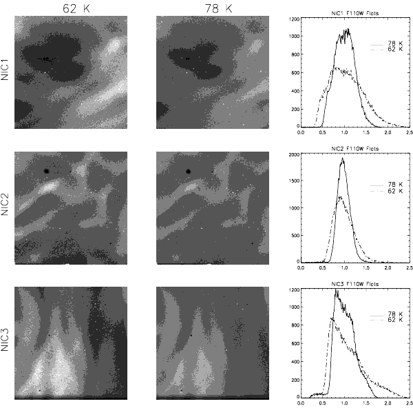
Read Noise
Each detector has four independent readout amplifiers, each of which reads a 128 x 128 quadrant. The four amplifiers generate very similar amounts of read noise. This is illustrated in Figure 7.10 which compares the pixel read noise distributions for the 1st and 4th quadrants of Camera 1. The distributions for all quadrants is relatively narrow, with a FWHM of 8 electrons. This means that there are only few very noisy pixels. The read noise does not change with temperatue.
Figure 7.10: Read Noise Characteristics for Two Quadrants on Camera 1 Detector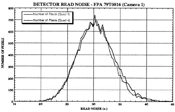
Linearity and Saturation
Until after Cycle 7, the linearity correction of the calibration pipeline had been based on the assumption that the NICMOS detector response was perfectly linear until count numbers reached a certain value, usually referred to as Node 1. No linearity correction was performed until this point was reached. The pixel was flagged as saturated when the deviation from the linear response reached 2%. This point, the so-called Node 2, occurs at about 90% of the full-well. However, an extensive Cycle 7 calibration program indicated that the detector response is in fact non-linear over the full dynamic range. For Cycle 11, a revised linearity correction will be implemented into the calibration pipeline which will correct data over the entire dynamic range of the defined saturaion level (Node 2). In other words, Node 1 will be set to zero. Figure 7.11 compares the new procedure to the one previously used. Here, we plot the response of a (arbitrary) NIC3 pixel, as derived from differencing subsequent readouts ("first differences").
Figure 7.11: Comparison between previous(dashed) and new (dash-dotted) linearity correction. The true pixel response is shown by the solid line.
|
Space Telescope Science Institute http://www.stsci.edu Voice: (410) 338-1082 help@stsci.edu |